1 Introduction
This document outlines the parameters which need to be measured
to ensure the array is operational and which can be used to check
continued expected performance of the array. There are two readout
modes of operation, STARE and NDR. The array needs to be characterised
in both these readout modes, if possible.
The following parameters need to be measured to fully characterise
the array-
· Bias Frames - Read Noise
· Photon Transfer
· System Gain
· Full Well
· Linearity
· Dark Current
· Other Quirks and Features
This document will outline how each of these parameters are
measured and give a description of the tools required. The user
is expected to have reasonable knowledge of how to use MICHELLE
and MICHELLE EXECs, IRAF and Microsoft Excel.
| |
System Gain |
Read Noise |
Full Well |
Non Linearity |
| Small Well |
~180 e/ADU |
~1000 e |
~7E6 e |
+/-2% |
| Big Well |
~ 500 e/ADU |
~2500 e |
~20E6 e |
|
|
2 Bias Frames
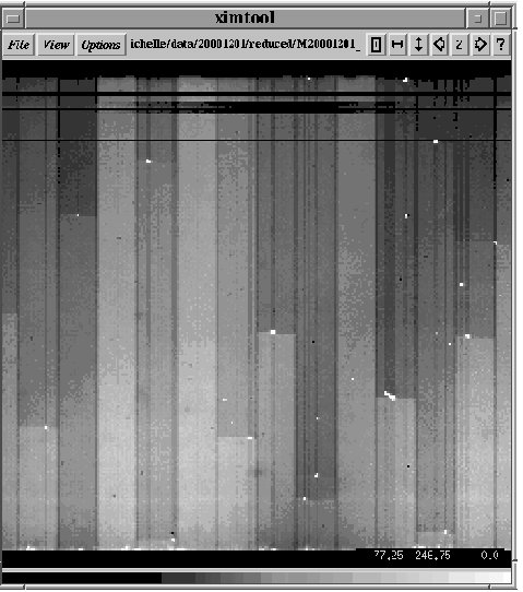
One of the first tests to do with the array is to take 2 simple
bias frames. These should be taken with the shortest exposures possible
looking at a cold blank. The following image shows a typical bias
image. Points to note are the following:-
· the array has 16 outputs, each region of the sixteen
240 x 20 pixels can be seen.
· the first 16th of the array has a lower bias level than
the rest of the array.
· note the row type defects across the top of the array.
· the bias level should be between 3000-9000 ADU depending
on waveforms chosen etc.
· note the hot pixels which then tail and also cause a
bias level offset to all the remaining pixels above
the hot pixel.
· check to see if there is any banding caused by mains
pickup etc.
|
|
|
3 Read Noise
To calculate read noise, take two bias images as shown above,
sbutract one from the other to remove the pixel non uniformity noise,
Divide the resultant image by root two. Then meaure the standard
deviation of the resultant in cosmetically clean regions of the
resultant image. This will be the read noise in ADUs of the array.
|
4 Photon Transfer - STARE readout
mode
Photon Transfer is the most powerful and important tool required
to fully characterise an array. It should be one of the first tests
performed to determine the overall health not only of the array
but of the array control electronics as well since this must be
in perfect working order for the photon transfer technique to work.
In its simplest form it is a plot of Signal versus Noise for the
array. We plot noise or the standard deviation as a function of
average signal for a group of pixels contained in the array image.
Data is plotted on a log-log scale in order to cover the dynamic
range of the array.
For a typical array there are three distinct noise regimes.
The first regime is the read noise floor which is the noise measured
under totally dark conditions, that is, the noise described above.
This noise is ultimately limited by the on-chip source follower
stages of the array. However it could also be due to other noise
sources which are independent of the signal.
As the illumination is increased to the array, then the noise
becomes dominated by the shot noise of the signal. This is the noise
associated with the random arrival of the photons on the array.
Some pixels intercept more photons than others which accounts for
the variance seen in pixel values for a flat illumination. This
process is governed by Poisson statistics which means that the uncertainity
of the quantity of charge collected in any given pixel is proportional
to the square root of the number of incident photons.
The third regime is associated with fixed pattern or pixel non uniformity
noise which results from sensitivity differences in each of the
pixels. These differences are caused by manufacturing processes
in which there are process variations, photo mask misalignments,
or whatever to cause each individual pixel to have a slightly difference
sensitivity the any other pixel on the array. Pixel non uniformity
noise is proportional to the signal.
To produce data for a photon transfer curve requires the following
steps :-
1. Determine the bias level of the array by taking exposures
in the dark with the shortest integration times possible.
2. Take 2 identical exposures with the same setup and integration
time. Repeat this process for many different integration times to
give a series of twin exposures which go from having very little
signal level all the way up to the saturation level of the array.
The Pixel Non Uniformity Noise can be removed by subtracting two
identical exposures thus the reason that two exposures are required
at each of the integration times.
3. Measure the Mean level from the average of the two exposures
taken at each of the integration times described above. Subtract
the bias level from these values to give the Mean Signal Level.
Do this for a particular region of interest (ROI) on the array which
is clean from any structure or artefacts.
4. Subtract each of the two identical exposures from each other
and divide the resultant image by root 2. Find the standard deviation
of the resultant image in the same ROI as used above.
5. Plot the Mean Signal Level against the Standard Deviation
for the ROI for all the different exposure pairs.
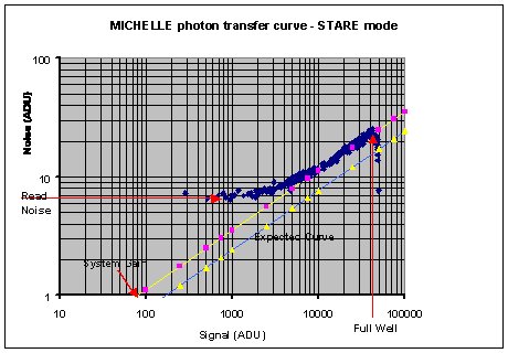
The resultant plot should look similar to the plot given below
for the MICHELLE array in STARE mode.
Points to note from this plot are as follows :-
· Where the curve flattens to the left of the graph is
the read noise of the array in Analog-Digital-Units (ADU). In this
example the read noise is approximately 5.5 ADU.
· In the main body of the curve where shot noise dominates
then the slope of the line should be 1/2. If we extend this line
of slope 1/2 back to the x-axis, see the yellow line with pink squares,
then the intercept of this line on the x-axis represents the system
electronic gain measured in e/ADU ( electrons per digital number).
In this example here this number would be approximately 80 e/ADU.
However the MICHELLE array suffers from excess noise which tends
to give a smaller value for this number than expected. See the detailed
description of this excess noise later in this document.The expected
shot noise regime is shown as a blue line with yellow triangles.
I have measured the system gain by other means to be approximately
170 e/ADU.
· Where the curve bends over to the right of the graph
gives a measure of the full well of the array. In this example it
is approximately 40k ADU.
From the example photon transfer plot the following system parameters
have been determined :-
Read Noise = 5.5 ADU
System Gain = 80 e/ADU but note the excess noise problem
Full well = 40k ADU
An "exec" script "array_tests" has been
written to produce all the required data to plot a photon transfer
curve. An iraf script has also been written, "stare_photon"
which takes the data produced by the exec script and plots a curve
as shown above. It also writes all the data, including exposure
time, signal, noise, gain and temperature into a text file. This
text file can then be read into Microsoft Excel. In Excel the data
can then be manipulated to produce photon plots and linearity plots
etc.
|
5 Full Well
As already stated the full well can easily be measured from
the photon transfer curve where the curve makes a sudden dive to
the x-axis. A simpler but quicker method is to look for the onset
of saturation of the array, visually. The number of ADUs at which
this occurs is then approximately the full well of the array. In
our array the full well is measured at approximately 40k ADU in
small well mode which equates to approximately 7 millon electrons.
|
 |
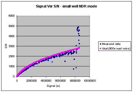
6 Note on Excess Noise measured
in MICHELLE array
As shown in the above photon transfer curve the system gain
measured by this method is not as expected. We believe that this
is due to excess noise in the array which is related to the signal
level. We also believe that the excess noise is a function of resetting
the array since as we shall see later on the Non Destructive Read
mode does not seem to suffer from the excess noise problem. Another
method of plotting to show the effects of this excess noise is as
shown below, a plot of Signal versus Signal/Noise for a specific
read noise, in this case 900e. An ideal plot is given together with
the results obtained from our array. The results obtained from our
array have also been replotted with the shot noise divided by root
2. This third plot fits the ideal curve more closely, but I as yet
do not understand the root 2 significance.
|
|
|
|
(Another device being tested by the Saclay group in France.
seems to suffer the same excess noise problems as our own array.)
To calculate the system gain we used the advertised values for
transimpedance supplied by SBRC in their manual and knowing the
electronic gain of the EDICT electronics we were then able to make
a reasonable guess of the system gain. To prove that this calculated
value for gain was the correct value instead of the value measured
by photon transfer required that we have some other method to determine
the gain independent from the above methods.
|
7 Independent method for system
gain determination
To perform an independent measure of the system gain we need
to be able to measure the current flow into the IR sensitive diodes
while integrating the array to a flat field source. To do this we
set up the acquisition system so that it is continuously taking
exposures which are, say, half filling the wells. We then monitor
the current flow to the Vdetgrv bias. To do this requires a scope
probe to be connected to this bias on the EDICT bias board, at Pin6
of the device, the other side of TP14. This is a very dangerous
operation and extreme care needs to be taken. We also need to monitor
and trigger on Vgate at the same time with a scope. As Vgate is
switched on then the voltage on Vdetgrv should change state in a
similar manner. In a example done in the lab, for 12ms exposures
(Vgate was ON for this time), we measured 38mV on the Vdetgrv bias.
With the current monitoring setup in the EDICT system, 38mV is equivalent
to 7.6uA. Now 1 A = 1Coulomb/s = (1/1.6E-19) electrons/s = 6.25E18
electrons/s. Then the electron rate here is 7.6E-6 x 6.25E18 = 4.75E13
e/s.
While doing this measurement we also need to store the images
produced and from them measure the number of ADUs in all the pixels
seen in the image. Again in this example we measured 3.1E9 ADU seen
in all the pixels in each 12ms exposure. This is corrected for the
bias. This then equates to 258E9 ADU/s.
The system gain is then given by 4.75E13 / 258E9 = 184 e /ADU.
This test was repeated for big well of the array and the system
gain was calculated to be 510 e/ADU. These results compare very
favourably with the numbers given in the SBRC manual.
|
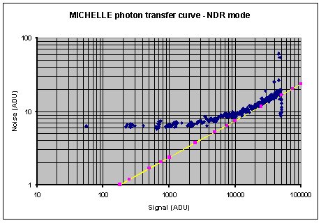
8 Photon Transfer - Non Destructive
readout mode (NDR)
The above photon transfer method was repeated but using the
non destructive readout mode. In this case the result images must
be multiplied by the read interval to give the real signal level
because the NDRE images always give the signal level normalised
to a 1 second exposure. The results for this test are as shown below.
|
|
|
The data for the above plot were produced with 2 Reads in the
Non Destructive Read Mode. In this mode the array is only reset
at the frame start and then the array is read out twice in a non
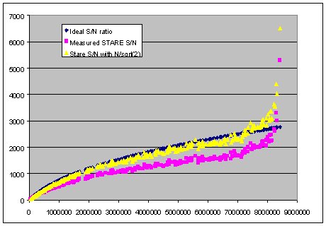
destructive manner. From the data we see that the S/N ratio of the
array approaches more the ideal S/N ratio than for the STARE readout
mode. The yellow line with pink squares is the case for an array
which is shot noise limited and has a gain of approximately 170
e/ADU. If we re-display the data in the format of S/N versus Signal
then we see that our NDR array data follows much more closely the
ideal S/N plot as shown below.
Again an "exec" script "ndr_array_tests" has
been written to produce all the required data to plot a photon transfer
curve. An iraf script has also been written, "ndr_photon"
which takes the data produced by the exec script and plots a curve
as shown above. It also writes all the data, including exposure
time, signal, noise, gain and temperature into a text file. This
text file can then be read into Microsoft Excel. In Excel the data
can then be manipulated
to produce photon plots and linearity plots etc.
|
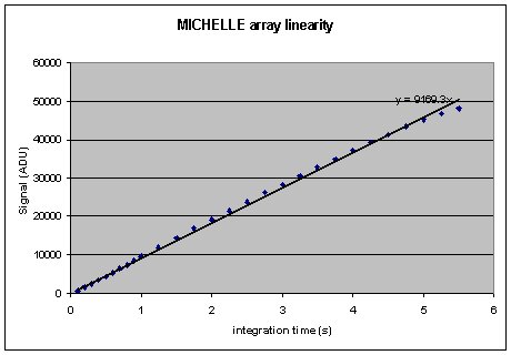
9 Linearity Measurements
The linearity of the array can be measured by simply plotting
integration time against mean signal level. An example of such a
plot is given below. The exec scripts and iraf tools for producing
such plots have already been described above.
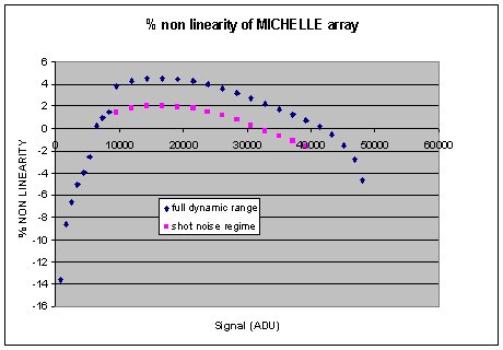
The second linearity plot shows the percentage non linearity of
the array compared to the trend line given in the first plot. The
array seems to be quite non linear. However the array suffers appreciably
from thermal affects where even reading the array out under different
regimes can cause the array to operate at different temperatures.
Looking at the temperature changes associated with this data set,
there was a 0.05K change from the first set of images to the last
set of images.
|
|
If we look at the percentage non linearity in the shot noise
dominated regime only then we see that it is approximately +/-2%
which is much more useable for science. This is shown in the second
plot as well.
|
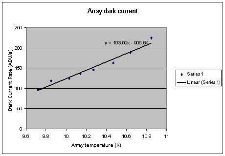
10 Array Dark Current
The ark current of the array cannot easily be measured whilst
the array is part of the MICHELLE instrument. This is because the
instrument itself is a source of background signal and it is impossible
to differentiate between background and array dark current. However
tests have been performed with the array looking at a cold blank.
The temperature of the array was then adjusted in small increments
using the local heater resistor. This heater resistor temperature
was then plotted against "dark current" rate for STARE
mode, small well, as shown in the graph below. The results shown
an dark current rate of approximately 100 ADUs per 1 K change in
temperature which equates to approximately to 17ke/K temperature
change.
|
11 Array Quirks
I have described in this section other know quirks and characteristics
of the array which have been seen in the lab at one time or another
but have not been characterised to any great degree.
|
12 Image Persistence
The array seems to suffer from persistence in that ghosts of
very bright objects can be seen in subsequent images even if they
are no longer being imaged. This persistence can be reduced by reading
out the array many times during the idle phases. As part of the
normal readout sequence idle clocks are run a few tens of times
before data is taken. This idle clocking can reduce the persistence.
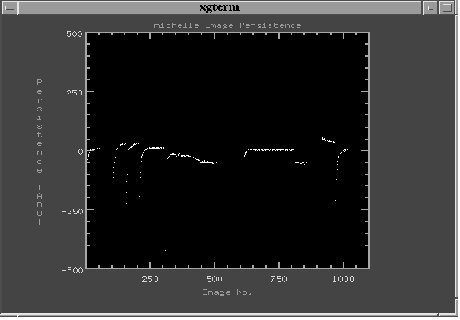
The above plot shows the effects of image persistence for the
array ranging from an image which was only at half full well to
an image which was ten times full well. To produce the above data
a bright slit was imaged onto the array. This was then removed an
a flat field was imaged onto the array. Many images were then taken
with this configuration to see if the slit remenance image disappeared.
The signal at the point where the slit was is then measured in relation
to signal in pixels either side of where the slit was. This is performed
for all the images taken after the slit image. We see from the above
plot that the slit persistence is below the flat field level. It
also takes a few tens of images for the persistence to disappear.
The persistence is also shown to be deeper the more we fill the
pixels or oversaturate the pixels. There is also an example where
the idle clocks are switched ON between slit and flat field images
and this shows a marked reduction in image persistence.
|
13 Temporal Noise
The system has been verified to ensure that there are no temporal
noise variations with the array. Basically a set of images have
been taken over a fixed time period of a few seconds. The standard
deviation of a group of pixles in time is then compared to the same
group of pixels in the spatial domain. There seems to be no increase
in noise over reasonably long timescales.
|
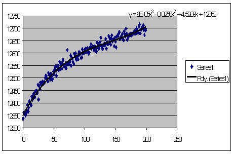
14 Readout Stability
The array seems to suffer from a problem where it takes at least
n reads of the array to stabilise, where n can easily be of the
order of a few hundred reads. If we continuously image a flat field
with the array and then plot Signal level against the image number
in the continuous read sequence then the following plot is seen.
If we run the idle clocking before any array readouts then the readout
stability can be much improved as seen by the second set of data
on the plot below.
|
15 Cosmetic Problems
The array suffers from many cosmetic features, in fact, at least
10% of the pixels are probably not scientifically useable. These
pixels fall into the first sixteenth and the last sixteenth regions
of the array. There are also many hot pixels scattered around the
array which affect the d.c. level of the remaining pixels in all
the rows above that pixel in that sixteenth region of the array.
There are also some rows near the top of the array which are scientifically
unuseable. These problems can be seen in the bias image shown below
:-
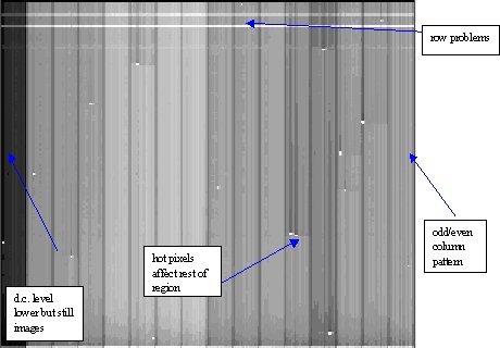
The level drop problem after a hot pixel will also be a problem
after bright stars.
|
16 Electrical shorts on the array
The gate of the cascode FET in the unit cell is drawing unusually
high currents (~240mA using nominal operating biases), where a good
array should not draw any current at all. Additionally, Vcap, the
"ground" side of the unit cell integration capacitors
is also drawing large currents (~3mA using nominal operating biases),
and should not be drawing anything. We characterized the shorts
by shutting off the DI gate (so that there was no contribution to
the measured currents from photo-flux or dark current) and sweeping
Vcasuc (with Vcap constant) and measuring the currents in PW, CAP
and CASUC, and then swept Vcap (with Vcasuc constant) and measured
the same currents. The currents are of opposite sign as measured
by the EDICT system, and give a power dissipation of ~15mW, which
is 20% of the total power dissipated by this focal plane and thus,
a suspect in the instabilities observed in this focal plane. All
the data support a short between Vcap and Vcasuc. I conjecture that
this short is (at least) partly responsible for the anomalously
unstable nature of this particular focal plane. In addition, we
checked to see if the short was sourcing or sinking spurious currents
that might appear as signal in the integration capacitor. We did
not find any evidence for this. We found that the low gain mode
drew considerably less currents than did the high gain mode, and
hence, that the array temperature was lower (by ~1K) in low gain
mode compared to high gain mode.
|
|
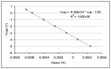
Characterization of the short between Vcap and Vcasuc indicating
a resistance of 6290W. The measurements were made under nominal
operating conditions with the direct injection FET gate shut off
(Vgate=-6V). The negative slope is presumed to be an artifact of
the current measuring sign convention.
|
|
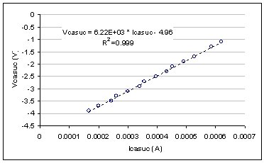
Characterization of the short between Vcap and Vcasuc indicating
a resistance of 6220W. The measurements were made under nominal
operating conditions with the direct injection FET gate shut off
(Vgate=-6V).
|
17 "Speckle Noise" Problem
The array also suffers from a defect known as the "Speckle
Noise Problem". A typical image showing this problem can be
seen below. The array noisier, or specklier at the top of the array
than at the bottom of the array. The problem cannot be seen in bias
images but only in images which have some signal in the pixels.
It also only manifests itself when we use the voltages for improved
QE performance and at the same time are very very short expsoure
times of the order of a few milliseconds. If we use longer exposure
times then the speckle pattern seems to go away. This problem may
be a function of the Vgate switch ON/OFF times and may be solved
by keeping Vgate on at all times.
|
|
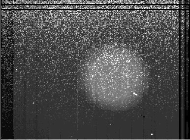
Speckle Noise problem
Notes on Big Well Performance
|